This is the final stage in the creation of a "brainless" microprocessor. By adding registers to our processor we will be able to process data. However, since we do not yet have a language to program our CPU with, we will need to manually set control switches. In the next section we will draw very heavily from here as we give our processor a 'brain.' However, for now let's first give our processor the memory it needs to compute.
So far we have only dealt with combinational logic. These are circuits whose outputs only depend on the current input. In this section we will introduce sequential circuits. Sequential circuits are circuits whose ouputs not only depend on the current input, but also on previous inputs. This ability to store information is an absolutly essential part to any microprocessor.
We will start with the most basic form of storage, a latch. A latch has an a single input, and a single ouput. It also has a control line. The ouput line always ouputs whatever value is stored in the latch. When the control line goes high, the latch takes whatever value is on the input line, and 'latches' (stores) it. Let's take a look at how one of these would look on a gate level:
[IMAGE UNAVAILABLE]
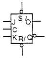
We won't actually use any latches, we will use their big brothers, Flip-flops. Flip flops behave very similar to a latch, only they store information when the control line changes from a 0 to 1. By only being activated during this transition, they get the name 'edge-triggered'. Put another way, it is not activated on a 0 or a 1, but rather during the transition time going from a 0 to a 1. This lets us precisely control when data is read into it. One of the most common flip-flops is a JK flip flop. A JK flip flop looks like:
Starting from the top, the S is a set line - whenever it is activated the FF gets a 1 put in it, the R is a reset - when it is activated a 0 is stored, the C is the clock to determine when data will be stored in our FF. The last input, J and K are the most important. If J and K are both 0 when the FF is told to get new data, it keeps the current value stored in the FF. If J is 0 and K is 1, it stores a 0. If J is 1 and K is 0, it stores a 1. And finally, if both J and K are 1's, it stores the inverse of the last stored value. The Q is simply the ouput, and Q bar is the inverse of the output. We will use this Flip Flop to build our first, and most important, memory -- a register. Let's take a look at the schematic we will use:
[IMAGE UNAVAILABLE]
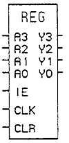
This register holds one bit of information. To load information into our register the input enable must be a 1, and the clock must make a transition from 1 to 0. When these both occur, a "snapshot" of the data on the data input is stored in the register. We'll combine 4 of these together to make our first 4-bit register, and represent it as:
The final extra bit we will need is a buffer circuit. A buffer circuit is a tri-state device that can 'break' a connection to a device. This will keep us from having more than one thing trying to use our databus at the same time. Think of it as a plug in a wall -- when we set our enable to low it "unplugs" the cable so neither a 0 nor a 1 is present. If it is high, our buffer's output asserts whatever value is coming into it. Since a 4-bit buffer is just 4 tri-state buffers, we'll just show the box view of it:
[IMAGE UNAVAILABLE]
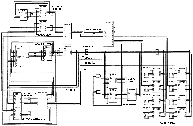
This makes up our complete memory, and buffer components. By simply connecting our ALU to a register, and adding a datbus to the memory we get:
Even though this circuit looks allot more complex it isn't. Most of what was added was enough memory to make the chip usable. Let's take a slow step through of what we've added. The bottom right of the circuit is the microprocessor memory. There are several types of memory here, RAM, ROM, and WOM (write only memory -- like a display). A closeup of the 4-bit ROM memory circuit looks like this:
[IMAGE UNAVAILABLE]
The keypad next to the buffer is the value that we have 'stored' in this memory. In an actual circuit this wouldn't be a keypad, but rather the binary lines would be tied high or low to make the value they wanted. An EEPROM found in development chips can be programmed repeatedly to change what lines are high or low, much like our keypad. In this circuit, when the 2 enables are high the data stored in the memory is put out onto the data bus. That buffer is there to assure that this ROM only asserts its data onto the bus when it is supposed to. Since we wish to only access this data when we are reading, we attach the read line to one of the enables. The other line is connected to the decoder, which selects the memory address for us. This also assures that only one memory will be accessing the bus at any time. This addressing procedure could be expanded as large as we need, but it follows the exact same pattern as we have here, just using larger decoders. Later on we'll add some more memory. If you look towards the center of the diagram, you can see a hex display, this is our output. Right before this is a register, this register is our Write Only Memory, or display WOM.
[IMAGE UNAVAILABLE]
On enable goes to the decoder, the other to the write line. When write is 1, data is being taken from the bus and put into memory. (Vice versa for when read is 1 -- read and write are never both 1). The most complex memory, our RAM, has components from both the ROM and the WOM. Data can be written into a RAM from the data bus, and then that data can be put back onto the data bus later. Since RAM can both read and write, it cannot share the same address with a rom or with an output. Let's look at the diagram for our ram:
[IMAGE UNAVAILABLE]
There is one very special register in our processor -- that is the one right next to the ALU. When you do a write to memory, this is the register that will put the data on the bus to be read by RAM. When you read data, the result coming out of the ALU will go into this register. This very special register is called the accumulator. For those of you already familiar with Intel Assembly language, this is reffered to as the AL register. On Intel's platform this is an 8-bit register, although our's is only 4.
Alright -- our brainless microprocessor is complete? But how does it work you say? Let's step through a basic addition procedure.