Our Arithmetic Logic Unit (ALU) is going to be our most complex building block. The ALU will have 2 4-bit inputs, and one 4-bit output. If our circuit is designed correctly, we can use the control circuits designed earlier to feed the inputs from memory to the ALU, and the output back out into memory. But let's not jump ahead just yet.
As you recall from our introduction to microprocessor theory, we need to have a set of commands for our microprocessor. These commands are simply a set of control signals fed into the ALU. The user's commands will contain the address of the memory location where the correct instructions are found. Also, we will want these instructions to be able to store the ouput in memory somewhere, so we need to design circuits that take a binary bit string and use it to activate only one output line. We will call these circuits Decoders.
This is the section where we have the widest space to expand our micro-processor. Our ALU will have all the basic functions, but there is no reason why we couldn't keep adding functions. These additional functions are what set the average processor apart from the outstanding processor. Of course, the more functions the processor has the larger the design, the more expensive to build. There is a very narow gate where we decide the time/money point where enough features have been implemented. For our processor we will add all the basic math functions, as well as the basic logical operations. If you wanted to take this processor further, spend some extra time in this section and add more functions to your processor.
Let's take a look at one of the very important parts we developed earlier, the two's compliment generator:
We are now going to make this device allot more powerful and give it several functions. These functions will include a 4-bit 2's compliment generator, a 1's compliment generator, and a passthrough. A set of select lines will let us choose which function we want the circuit to perform. Let's take a look at the function table that we will use to control this chip:
  ___       ____
  NEG/NOT | PASS |   Function
 ---------+------+--------------
     0    |   0  | Pass-through
     0    |   1  | Two's Comp.
     1    |   0  | Pass-through
     1    |   1  | One's Comp.
As you can see, anytime the pass line is 0, the chip sends the input to the ouput, and anytime it is 1 the value of Neg bar/not determines the function. Here's the schematic that gives us those fuctions from our little 2's compliment generator:
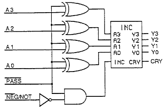
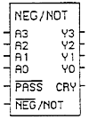
Let's now take that NEG/NOT chip and place it into a box for use as a building block in our ALU:
That is the first major component of our ALU. Let's dive right into the next one, the ADD/OR circuit. If you think about it, using the building blocks we've already built this circuit is child's play. We have 2-4bit inputs, and one 4-bit output. We want to be able to add them, or 'OR' the 2 signals. How would we add them? By using the 4 bit adder we developed. How would we 'OR' them? Simple, by using 4-OR gates. Now, if we connect the inputs to both of these circuits at once, we will have 2-4bit outputs, one with the OR result, the other with the 'ADD' result. Remember that 4-bit Multiplexer we designed? I hope so, because we will just add that to the end of the circuit to decide which answer we will pass on! Let's take a look at this simple circuit:
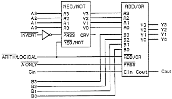
Re-iterating, this circuit performs both the Add and the Or, and then using the multiplexer control line you decide which answer will go to the output lines. These two functions are nice, but it is also very handy to have a pass-through on our circuits, so we'll just add that into a second multiplexer. Now the circuit is an ADD/OR/PASS circuit, looking like:
Just to keep things straight before our circuit gets too large, let's take a look at the function table for this chip.
  ___      ____
  ADD/OR | PASS |   Function
 --------+------+-------------
     0   |   0  | Pass-through
     0   |   1  | Add
     1   |   0  | Pass-through
     1   |   1  | Or
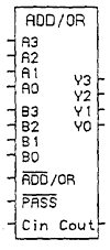
Let's put this powerful circuit into a box, to be a major component of our ALU.
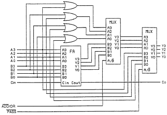
Let's take these circuits we've designed and put them together into an ALU now, our largest building block in our Micro-processor. At this point, our ALU has the ability to perform 1's compliments, make a 2's compliment, Add, or, and pass through data. These functions can be combined in our instruction set to make more complex instructions like a subtract function that first converts a numer to two's compliment, and then adds it. So let's take a look at our ALU circuit that we've developed:

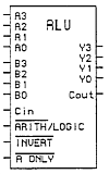
Now, let's finalize the building block process by placing this ALU into a box:
Our Microprocessor is at a good point to take a moment and discuss where we could really make this chip powerful. In the modern world, a 4-bit chip wouldn't get you very far. Howerver, think of how you would build an 8, 16, or 32 bit chip. Let's take our adder for example. We started with a 1-bit adder, connected 4 of them, and made a 4-bit adder. Now that we have a 4-bit adder, we could connect 2 of those and make an 8-bit adder. With an 8-bit adder, we could connect 2 of those to get a 16-bit adder. Now, connect two of those and you have your powerful 32-bit adder. There is no reason why our design could not be very easily scaled up to a 32, or 64-bit design except for time and space. If you take this building block approach, a 64-bit adder is not that complex a thing. However, if you tried to tackle the entire project all at the same time, you might lose your mind in all the AND/OR/INVERTER gates staring at you. Every once in a while it is worth evaluating your circuit to see if there are ways you can optimize it further. Especially if your chip is going to be used for a high speed leading edge design. There are computer programs available that will search for removable gates in your circuit, and reduce the size. Or, you can take the entire circuit project into a Karnaugh map, and optimize it by hand. The ability to just use a K-map will vanish very shortly however, when we add memory and sequential circuits into the mix. Why worry about the chip count? Other than straight cost, every gate that you put in a circuit adds a small delay until the signal can be processed. Although for only a couple gates this time is negligible, when you start creating complex circuits like ALU's that go through many gates, you must keep the clock speed of your processor slower than the time it takes all of the gates to propogate. This explains the difference in machines like the SNES which can only operate at 3 MHZ, and the new Ultra-64 which can operate at 93 MHZ. The u64 processor is a lesson in good processor design. SGI has always been known for some of the best CPU designs in the industry.
Back to building, let's take a turn from adding new functions to our processor to making the glue that will hold all of our pieces together. The first is a Decoder. A 1-bit decoder is actually just a demultiplexer, but since it is used for a different purpose, we rename the in and out lines. Decoders are used to activate a specific memory location. They do this by taking the binary input number, and then putting a 1 on whichever line is specied, and 0's on every other line. The decoder also has an enable line. If this enable line is ever a 0, the decoder is turned off and all lines output a 0. This is important when we stack decoders to make more memory addresses avavilable. Let's take a look at using this 1-bit decoder to make a 2-bit decoder:
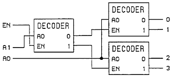
Which behaves according to this truth table:
 EN | A1 | A0 || 0 | 1 | 2 | 3
 ---+----+----++---+---+---+---
  0 | 0  | 0  || 0 | 0 | 0 | 0
  0 | 0  | 1  || 0 | 0 | 0 | 0
  0 | 1  | 0  || 0 | 0 | 0 | 0
  0 | 1  | 1  || 0 | 0 | 0 | 0
  1 | 0  | 0  || 1 | 0 | 0 | 0
  1 | 0  | 1  || 0 | 1 | 0 | 0
  1 | 1  | 0  || 0 | 0 | 1 | 0
  1 | 1  | 1  || 0 | 0 | 0 | 1
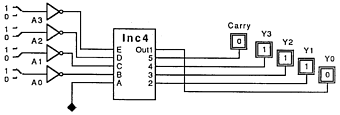
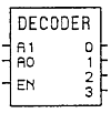
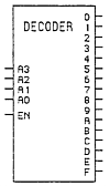
Now, let's just expand that to make a 4-bit decoder for use with our processor. And we'll label that in a box as:
And building still further, we get:
This marks the end of all of the combinational logic circuits that we will use in our processor. However, there is allot more to come in the form of sequential circuits. These are the circuits whose output is directly dependent on not only their input, but their current output as well. Join in for the next segment as we cover buffers, registers, and our basic memory.
Jump Back to the Processor Design Home Page