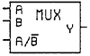
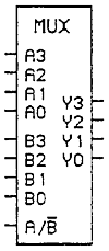
A microprocessor that can't change the way data flows through it is useless. Therefore, we need to design a circuit that will let us route data through our chip. Such a device is known as a Multiplexer. A multiplexer has two data inputs, one data output, and a select line. Depending on whether the select line is high or low either the data from input 1, or input 2 is shown on the output line. In our multiplexer, we will call input 1 A, input 2 B, the select line C, and the output line Y. Let's first look at the truth table that I've just described:
    A | B | C | Y
   ---+---+---+---
    0 | 0 | 0 | 0
    1 | 0 | 0 | 0
    0 | 1 | 0 | 1
    1 | 1 | 0 | 1
    0 | 0 | 1 | 0
    1 | 0 | 1 | 1
    0 | 1 | 1 | 0
    1 | 1 | 1 | 1
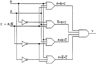
As you can see, it only has three inputs, that affect a single output. Remember those Karnaugh maps from earlier? Well, now is the time to use them. There are several implementations of this possible, so if you develop a different one, feel free to use it. This POS implementation's schematic looks like:
Now let's put that multiplexer into a box to use as another building block, giving us:
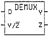
This is a very usefull circuit we have just designed, but it is not the only control circuit that we need. At times we will have one data input, and want to route where it goes. We call this a demultiplexer. Go ahead and design this one on your own, it is pretty simple. Just to be clear, here is the truth table. Remember in this circuit D is our input, Y/Z bar is our select, Y is output 1, and Z is output 2.
          _
    D | Y/Z | Y | Z
   ---+-----+---+---
    0 |  0  | 0 | 0
    1 |  0  | 0 | 1
    0 |  1  | 0 | 0
    1 |  1  | 1 | 0
We'll use the building block representation of this circuit here:
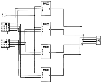
These are nice, but a 1-bit anything isn't too useful in our circuit. Therefore, just like we did with the adder, we will combine several of our multiplexer1 circuits together to make a 4-bit multiplexer. Remember, to control the four inputs we only need 2 select lines, in binary this gives us 4 combinations 00 01 10 11. This is known as addressing. In fact this is the basic scheme that all computers use to route information, and how we will talk to specified memory later on. Well, let's take a look at our new 4-bit multiplexer:
Okay, this gives us some good control circuitry now. We will use this control circuitry in our ALU. Let's jump to the next section and design some basic logical operation circuits, and combine them all into an ALU.
Jump Back to the Processor Design Home Page